
I spend more time than I probably should reverse engineering circuit boards, so I figured I would write up a page on how I do it. This only applies to two sided PCBs, and requires some time of imaging device, photo editing software, and your favorite PCB layout program. I use a flatbed scanner, Photoshop, and KiCAD. The basic steps start with getting pictures of the PCB with all components, getting pictures of the PCB without any components, using Photoshop to make a drawing of the traces, and finally bringing it all into KiCAD for the final schematic. It’s a long process and I hope someone can come up with a better way, but until then here goes nothing
Take as many pictures as possible during all steps. The last thing you want is to disassemble the PCB and realize you didn’t mark where a certain resistor went.
Imaging the PCB
There are three ways that I have tried to get a picture of the PCB, and by far the best way is a halfway decent flatbed scanner. I used to use my phone, but the lighting was an absolute pain and would cause issues where I couldn’t see some traces so I came up with a little lightbox. The lightbox is just a white box with a bright LED in it, and a hole cut for my camera. The PCB is held to the wall using a thumb tack and some clay – it was a truly professional set up (sarcasm, obviously).
I then used the same ligthbox but with a DSLR – this gave slightly better results, but it was an older DSLR and not quite worth the resolution loss. It was necessary to use a tripod and timer, because the small shake from actually pressing the shutter button was enough to make the picture not optimal.


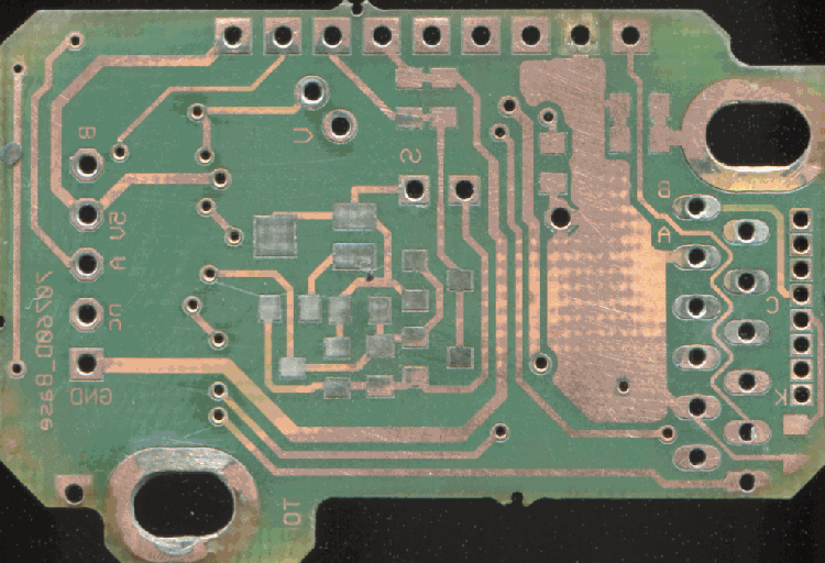
Here are the results of scanning – I had to remove some SMD potentiometers to make sure the PCB was flat on the screen, but other than that and some basic acetone cleaning, nothing was needed.


I put both images in photoshop, and slight them using the via holes and assign components references (R1, R2, etc). See the gif below. I’m not planning on doing a photoshop tutorial for a few reasons – one, I suck at photoshop. Two,

Removing Components


Keep track of which component is labeled what. It is hard to tell the difference between some SMD capacitors and SMD inductors, and whether that SOT23-3 is a dual diode, transistor, etc, so make your best guess. As long as it has a label. I then go through and try to figure out as many components as I can – some components are easy like resistors and the bigger ICs, but some of the smaller components have very few if any markings. Sites like this https://www.random-science-tools.com/electronics/SMD_markings.php can help – one of the SOT23 parts just said “3F” on it – turns out that means it is a BC857B PNP transistor. For the capacitors and inductors, you’ll need a multimeter capable of measuring them, and some way to probe the leads. You have to take the components off before measuring them if you want accurate results. Enter these little tweezers I printed from here https://www.thingiverse.com/thing:2145253

Tracing the Traces
This part is the most straightforward – I just scanned the PCB after removing all components. The picture below is from one I sanded down, because that was almost necessary when using my phone. The flatbed scanner gets consistent enough lighting that the sanding is unnecessary.

And back to photoshop
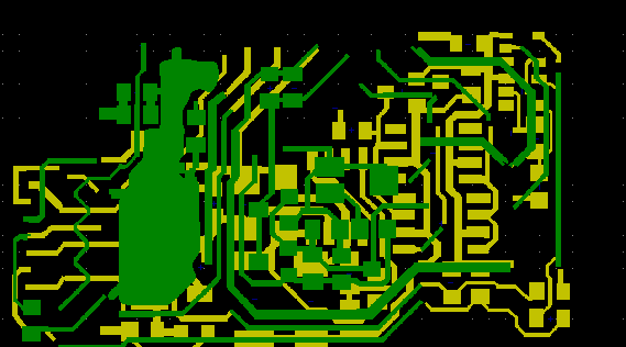
The last thing I do is export the traces to a bitmap, which can be imported to KiCAD footprints. I bring the top layer in to Eco Block 1, and the bottom in Eco Block 2. I also use the holes/vias on a separate layer.
KiCAD
After importing the bitmaps as footprints, I lay them out in the correct positions like so:

I then start adding components and aligning their footprint to the images, connecting traces, rinsing and repeating. It is long and tedious, but if followed correctly you won’t miss any traces.
And the final schematic:

My next post will hopefully be designing a dynamic torque sensor 😉