
I want to build a DC power supply for my electronics workstation desk that has 3.3V, 5V, 12V, -12V, and 0-24V adjustable outputs. I’ve been learning quite a bit about power supplies over the last few days, so hopefully I can make something that is somewhat efficient and won’t blow up. Assuming I actually get this power supply to work well, I will be posting the Eagle files and a BOM to get the parts necessary to build it. This page covers the basic voltage converter schematics, and the next page will cover the current sensing part of the circuit.
Table of Contents:
AC to DC Converter
The first step is obvious: I need to convert 120V AC to a DC voltage. Now it might make sense to drop the 120V AC to 24V directly since that is my maximum output, but since I want some stability in the voltage I think I need to drop it to around 36V, then to 24V. Let’s narrow down the specs a little more:
- 3.3 and 5V rails should supply 1A each
- +12V should supply 4A
- 0-24V should supply 4A
- -12V should supply 1A
This gives us a maximum power usage of (3.3V * 1A) + (5V * 1A) + (12V * 4A) + (12V * 1A) + (24V * 4A) = 164.3W, so a 200W power supply would be sufficient. I toyed around with the idea of making my own converter, but then I quickly realized I am a mere mortal and it is well beyond my grasp. Perhaps in the future. Anyways, here’s this:
36V Switching Power Supply from Automation Technologies
I’ve ordered stuff from them before and was not disappointed.
DC to DC Converter
Using the specs mentioned earlier, I used Texas Instrument’s WEBENCH Power Architect to generate some designs that should do exactly what I want. I won’t go through that whole process because it is a bit of a nightmare, but I basically kept clicking until I had some design. Unfortunately, it was fairly difficult to just copy the designs into Eagle – there were some weird compatibility issues – and it was annoying trying to make a BOM for Digikey. So I figured I might was well design each part of the DC-DC power supply from scratch – great learning opportunity.
3.3V 1A Output
The IC that WEBENCH recommended was the LMZ14201. This is a synchronous buck converter module that allows up to 1A output, and 6-42V input. Looking at the application example in the schematic:

The first section in the “Detailed Design Procedure” states that the Enable line can be connected to Vin by the voltage divider circuit shown in the schematic. Basically the goal there would be to automatically enable/disable the circuit when the voltage at the EN pin reaches the threshold (about 1.18V). However I plan on using a microcontroller to deal with enabling the power supplies, so I can eliminate Rent, Renb, and D1. One thing to remember though is the EN pin is internally pulled HIGH, so I’ll need to add a pull-down resistor otherwise the output will be always on.
Output voltage is determined by Rfbt and Rfbb – this creates a voltage divider that interestingly enough alters the PWM cycle times of an internal MOSFET – this is what changes the output voltage. The equation is:

And the resistors must be chosen from  to
to 
Cff is a feed forward capacitor that improves the load step transient response – this value is “usually determined experimentally by load stepping between DCM and CCM conduction modes and adjusting for best transient response and minimum output ripple” – but the table below shows some appropriate values.

This module allows for a “soft-start” which basically just slows the increase in voltage output once the EN pin is pulled high – this limits the amount of instantaneous current needed. Css is the capacitor that determines this, and the equation is

When  and is the minimum recommended value.
The Co capacitors are used to reduce the output voltage ripple, and  is the minimum while TIs demo and eval boards have a
  6.3V X5R capacitor. This capacitor should be a ceramic capacitor or something else with a low ESR (equivalent series resistance).
Cin limits input voltage ripple. In this case, the minimum recommended capacitance is X7R with a voltage rating 25% higher than the maximum input voltage. Strangely, the capacitor isn’t picked by capacitance, but by the input ripple current rating which is given by:

Now there is something wrong with this equation, because it tries to take the square root of a negative number, so we will just move on for now. I copied it straight out of the datasheet so who knows.
There are a few other values that can be calculated, but fortunately there is a table with recommended values:

This is even setup for 3.3V! So here’s a quick schematic I made:

And here is a quick summary of the PCB layout guidelines:
- Place Cin1 as close as possible to LMZ14210 VIN and GND pad
- LMZ14210 GND pad should connected to top side GND plane that also connects input and output capacitors
- Single point ground – connect the GND pin and the GND pad directly
- Minimize trace length to FB pin
- FB pin copper area as small as possible
- Rfbt Rfbb and Cfff should be routed away from LMZ14201
- Input and Output bus connections wide as possible
- Adequate Heat Sinking – use array of heat-sinking vias to connect exposed pad to the ground plane on the bottom PCB layer – 6×6 via array with minimum diameter of 8 mils spaced 59 mils
Here is an example PCB layout

And here is a quick one I made – although I won’t be getting this board manufactured since I want to combine all of these power supplies into one board, I just did this for practice:

Aside from the silkscreen containing letters where I need to solder, this circuit should work pretty well.
5V 1A Output
Here I am going to do the exact same circuit as the 3V3 supply, except changing the values of Rfbt and Rfbb to get 5V. Values of 5.62k and 1.07k should work, as per the table shown earlier. But now, I’m going to combine the circuits.

As you can see, the schematic is now prepared to handle the rest of the supplies, and organized a little better. Eventually I want to add in a current monitor, so the Controller Connector will need to have more pins. I’m not going to mess around with designing a board this time, instead I’m going to move on to the 12V supply.
12V 3A Output
Going to the LMZ14203H datasheet reveals this example schematic:
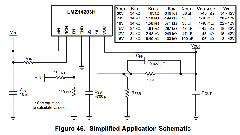
Look familiar? The equations are largely the same (make sure you check the datasheet first), so here’s my updated schematic:

24V Supply
Lucky me, this can be done with the same IC so I just need to change the resistor values like so:

-12V Supply
This one is tricky, I am using the LMZ34002rKGR switching converter. Using TI WEBENCH, I made the following schematic:

This includes the DCX114FH-7 level translator. It is kind of a nightmare, to be honest. I don’t think I’ll be adding a current monitor to this circuit, because negative voltages are such a pain.
Final Schematic
Here’s the final schematic before adding the current sensing and stuff.
